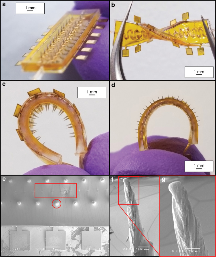
Fig. 7. Optical and SEM images of packaged and assembled µserpentine sensor device.
a Optical image of the fully assembled 3D microelectrode device, schematically represented in Fig. 1. b Optical image of the microelectrode µserpentine device undergoing twisting with a pair of tweezers. c Optical image of the 3D µserpentine microelectrode device undergoing end-to-end bending. d Optical image of the microelectrode µserpentine device in a reverse cuff conformation, exposing the microelectrode needle tips for imaging. e SEM image of the fully assembled device. The highlighted regions denote where the laser isolation trace is located beneath the PDMS layer (and hence are difficult to visualize) and where the exposed circular electrode tips emerge from the PDMS layer. f SEM image of the exposed electrode tip. After insulation, it is estimated that the electrode tips are 300 µm in height above the surface of the PDMS. g SEM close up of the electrode tip from f, highlighting the naturally formed µSLA striations, which contribute to the increased effective surface area of the 3D microelectrode.

