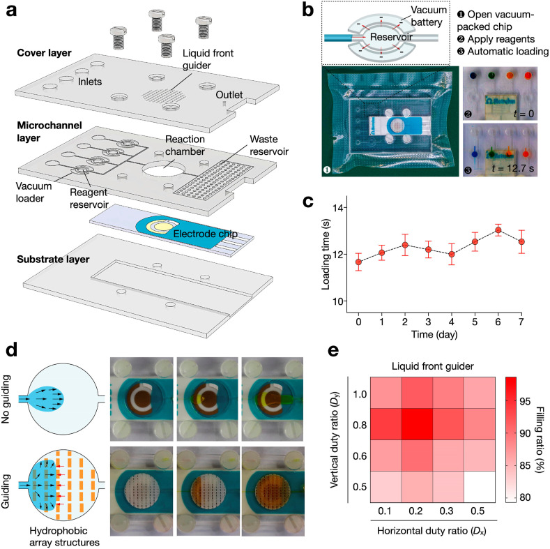
Fig. 3.
Microfluidic chip design.
(a) Exploded view of the chip. It consisted of two PMMA layers (cover and substrate layer) and a PDMS layer (microchannel layer) to embed the nanostructure-functionalized electrode. The layers were attached together with silane bonding and screw-actuated clamping. (b) Vacuum loader to automatically transfer reagents from inlets to the on-chip reagent reservoir. This design eliminates any possible contact between reagents and the pumping system, so as to minimize carryover contamination. (c) Time needed to load reagents into the reagent reservoirs (i.e., loading time) as a function of the storage time in vacuum packing. (d) Liquid front guider to improve fluid filling. Laser-engraved pillar array was implemented on the roof of the reaction chamber to form multi-layered perforated barriers perpendicular to the fluid flow. In the absence of the guider, when a liquid is filling a large chamber, it spreads naturally with a small divergence angle and leads to bubble retention. When the chamber is equipped with the guider, the liquid spreading is regulated to ensure complete filling. The liquid is guided to move between two pillar layers, due to a smaller resistance. Once the void between the two layers is completed filled, the liquid breaks the capillary resistance to fill the next interlayer space. (e) Filling ratio with different geometry of liquid front guider. The guider demonstrated the best performance when the horizontal (Dx) and vertical (Dy) duty ratios are 0.2 and 0.8, respectively. All measurements were performed in triplicate. In c, the data are presented as mean ± s.d; in e, the data are presented as mean.

