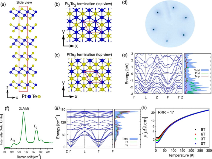
Figure 1.
(a) Side view of the layered Pt3Te4 crystal structure, with alternate PtTe2 and Pt2Te2 layers stacked along the vertical direction. Panels b and c show the top view of the Pt3Te4 surface with (b) Pt2Te2 and (c) PtTe2 terminations, respectively. (d) LEED pattern obtained at an energy of 100 eV. (e) Band structure and the corresponding density of states. (f) Raman spectrum acquired using a laser with 632.8 nm wavelength. (g) Theoretical phonon dispersion in the primitive unit cell along with the phonon density of states. (h) Resistivity as a function of temperature, for four different values of the magnetic field, ranging from 0 to 9 T.

