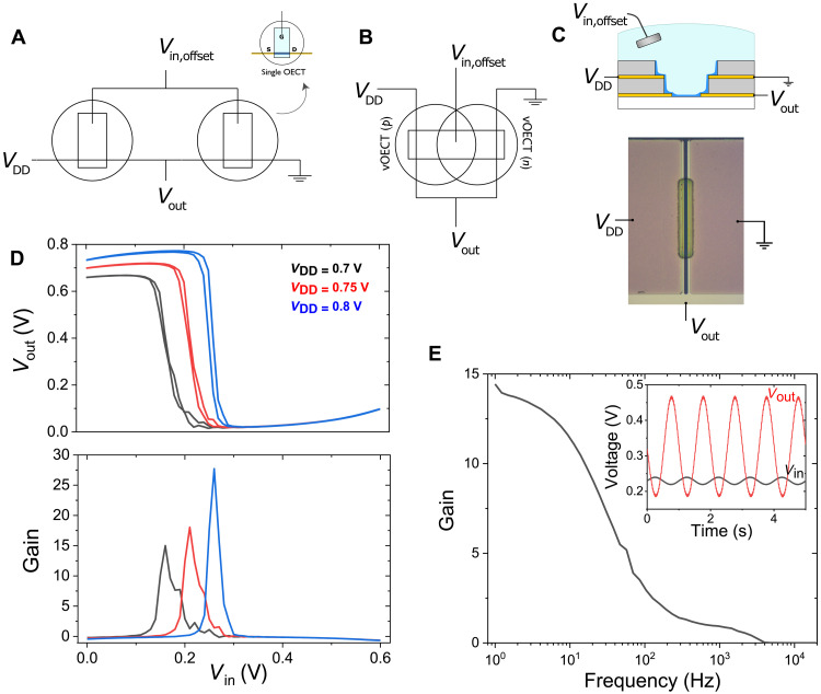
Fig. 2. OECT cofacial pair complementary inverter.
(A) The wiring diagram for an OECT-based complementary inverter with two OECTs independently gated. (B) The condensed wiring diagram of an OECT complementary inverter based on a cofacial pair of vOECTs. (C) Schematic cross section of a cofacial pair wired as a complementary inverter and a top view microscopic image of the cofacial inverter. (D) The voltage transfer characteristics (VTCs) of the cofacial pair inverter (ΔVin = 0.01 V; 0 to 0.6 V; and VDD = 0.7, 0.75, and 0.8 V). The corresponding gain (δVout/δVin) with peak gains of 15, 18, and 28 for VDD = 0.7, 0.75, and 0.8 V, respectively. (E) The frequency response of the cofacial pair. The inset shows a sinusoidal input (ΔVin = 0.01 V with an offset of 0.23 V at 1.5 Hz and VDD = 0.8 V) with the corresponding amplified output.

