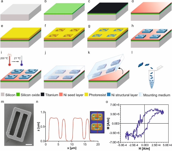
Figure 2.
Technology development of the Ni barcodes. (a) A silicon wafer substrate as the starting material for the fabrication of the magnetic barcodes. (b) 1 µm of silicon oxide was deposited. (c) A 50-nm-thick of Ti and (d) a 50-nm-thick of Ni were evaporated as metallic seed layers. (e) 0.9 µm of photoresist was spun over the surface. (f) Patterned photoresist after exposure to ultraviolet light through a photolithographic process to get the inverted barcode pattern. Barcode devices were fabricated from the inverted photoresist pattern. (g) 1 µm of Ni was deposited with the electroplating process. (h) Removal of the photoresist. (i) Thermal-shock was performed after heating the devices at 200 °C for 20 min and followed by a quick cooling down to room temperature. (j) A drop of an aqueous mounting medium was cast over the devices. (k) Manual peeling of the solidified membrane was performed to release the barcodes. (l) Chips were collected in an Eppendorf by dissolving the membrane in water. (m) SEM images of a Ni fabricated barcode with code number 0000–0000 = 0, after its release. Scale bar: 2 µm. (n) Confocal profiles of Ni barcodes (right inset shows the scanned line), z represents the vertical dimension and x the length along the scanned line. (o) Hysteresis loop of Ni barcodes measured with a VSM for magnetic characterization. M represents the magnetization and H is the applied magnetic field.

