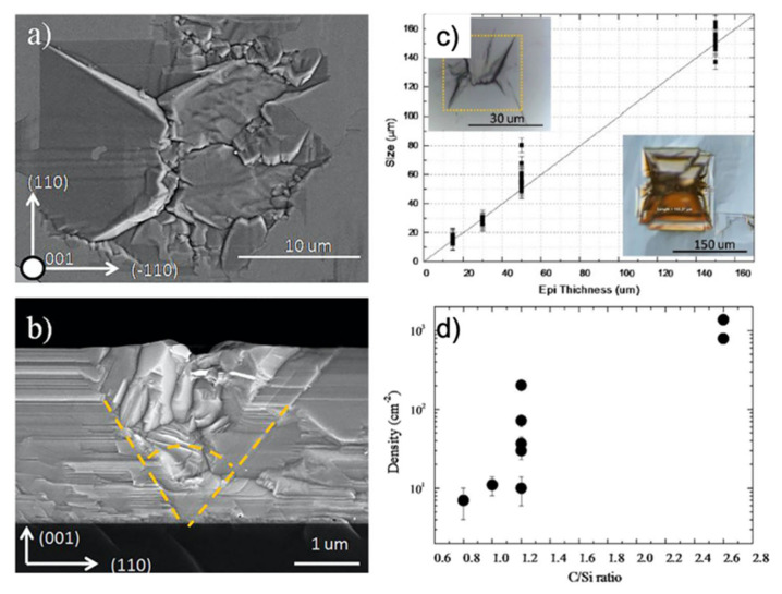
Figure 17.
(a) Scanning electron microscope plan-view image of a protrusion in a 30 μm-thick epitaxial layer. (b) Cross-view obtained after the cleavage of the wafer for a 3 μm-thick epilayer. Yellow lines are drawn in order to identify the edge of the defect. Crystallographic orientations are also drawn. (c) The average size of the protrusions vs. the epitaxial layer thickness. (d) The density of the protrusion as a function of the C/Si ratio during the buffer layer step (adapted from Reference [67]).

