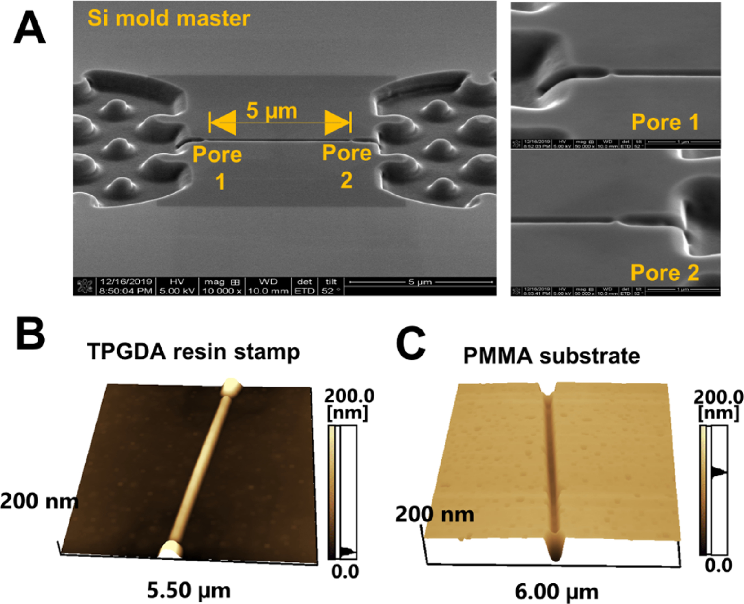
Figure 1.

Dual in-plane nanopore device. (A) SEM image of the Si mold master. The two in-plane nanopores are 5 μm apart from each other. AFM scans of the (B) TPGDA resin stamp and (C) imprinted PMMA substrate. Tapping-mode AFM scans were acquired at 0.5 Hz scanning frequency using a high aspect ratio tip with a radius of <2 nm.
