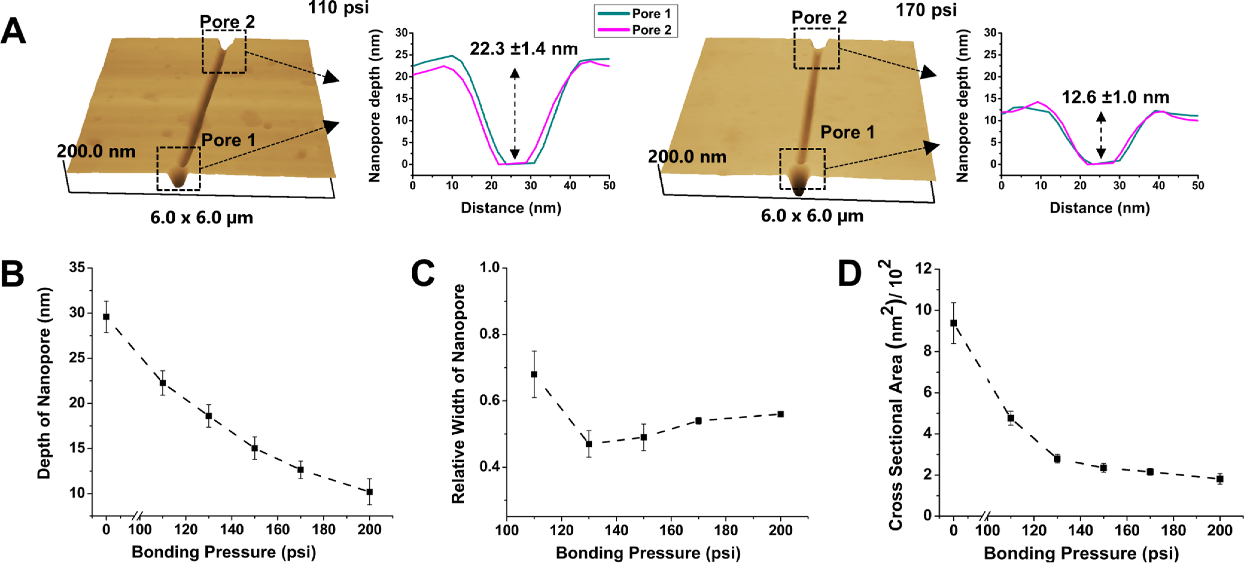
Figure 2.

Nanopore depth and width with varying thermal fusion bonding pressure. (A) AFM scans of PMMA devices at 110 and 170 psi bonding pressures. (B) Change in the depth of the in-plane nanopores with bonding pressure. (C) Relative width of the in-plane nanopores after bonding at different pressures relative to the width of the nanopore before bonding (0 psi). There was no statistical difference in relative width from 130 to 200 psi at the 95% confidence interval (p > 0.05). (D) Cross-sectional area of the in-plane nanopore with thermal fusion bonding pressure.
