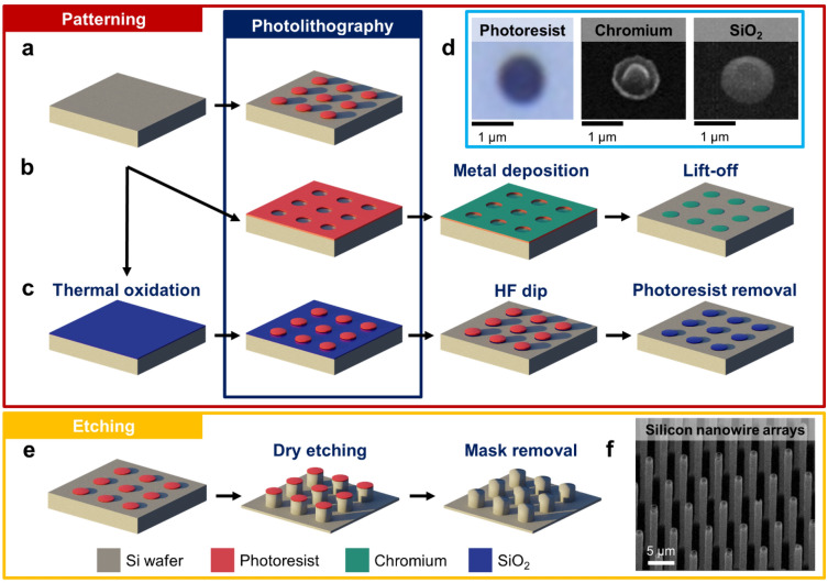
Figure 1.
Fabrication routes of vertical silicon (Si) nanowire arrays using different mask materials. Patterning of (a) photoresist, (b) chromium (Cr), and (c) silicon dioxide (SiO2) masks combines photolithography and several thin-film fabrication techniques (i.e., electron-beam evaporation for Cr thin film and wet thermal oxidation for SiO2 thin film). (d) The resulting photoresist, Cr, and SiO masks on Si substrates showing circular patterns with a diameter of ~1 µm. (e) Inductively coupled plasma reactive ion etching (ICP-RIE) process of pre-patterned Si substrate yielding vertically aligned Si nanowire arrays. (f) Scanning electron micrograph of the fabricated vertical Si nanowire arrays.

