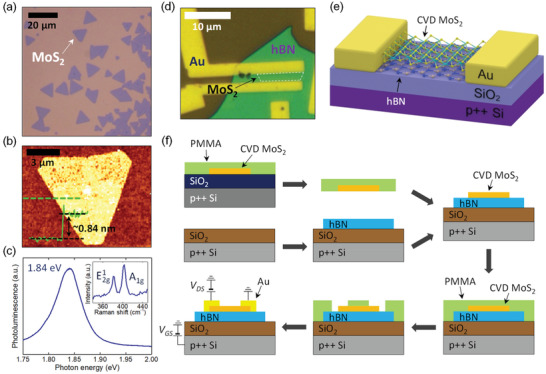
Figure 1.

a) Optical image of CVD‐grown MoS2. b) AFM image of a CVD‐grown MoS2 flake with its topographic cross‐sectional profile across a green dashed line. c) PL and Raman (inset) spectra of MoS2. d) Optical image of a representative MoS2 FET fabricated on a hBN flake. e) Schematic of the fabricated MoS2 FET with Au contact. f) Fabrication procedure of MoS2 FETs.
