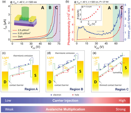
Figure 3.

a) I DS measured in the dark and under the laser irradiation with different irradiation intensities. V DS was swept from 0 to 72.75 V with a step of 0.25 V. The inset shows a schematic illustration of laser irradiation to a MoS2 FET. b) Photoresponsivity and detectivity calculated under the irradiation with the intensity of 0.23 µW cm−2 versus V DS. The inset shows the photoresponsivity (R) of the same device calculated under the irradiation with the intensity of 2.5 µW cm−2 at V DS from 0.25 to 2.5 V. Schematics of energy band diagrams in the off state of MoS2 FETs in the c) region A, d) region B, and e) region C. Red and blue symbols indicate electrons and holes, respectively. S and D denote source and drain, respectively. Two colored bands (bottom) indicate the V DS region where carrier injection and avalanche multiplication are weak (blue) or strong (red), respectively.
