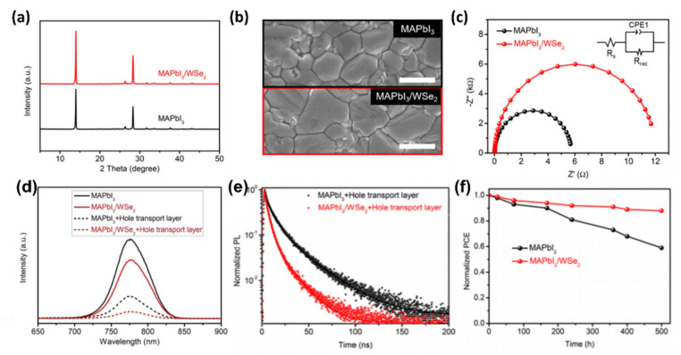
Figure 6.
(a) XRD patterns of MAPbI3 and MAPbI3/WSe2 films; (b) SEM images of MAPbI3 and MAPbI3/WSe2 films; (c) Nyquist plots of MAPbI3 and MAPbI3/WSe2-based PSCs; (d) PL spectra of the MAPbI3 and MAPbI3/WSe2 films with and without hole-transporting layer (HTL); (e) TRPL decay curves of the MAPbI3+HTL and MAPbI3/WSe2+HTL structures; (f) Photostability of non-encapsulated MAPbI3 and MAPbI3/WSe2 based PSC devices under storage in N2 glovebox (illumination of 100 mW cm−2 white light-emitting diode (LED) for 500 h). Data taken from ref. [86]. Copyright American Chemical Society@2021.

