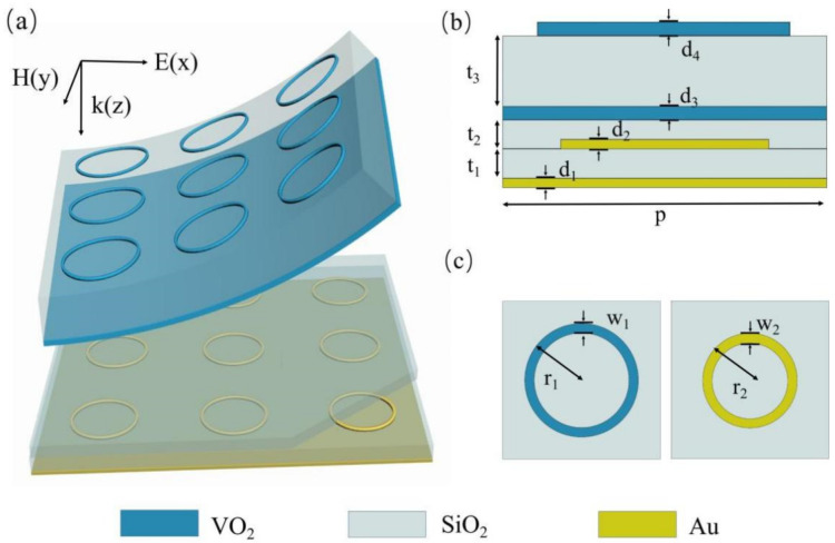
Figure 1.
(a) Schematic of the proposed multi-band absorber. (b) Side view for one unit cell of the multi-layer composed structure. The detailed parameters are p = 85 µm, t1 = 6 µm, t2 = 5 µm, t3 = 20 µm, d1 = d2 = 0.4 µm, d3 = d4 = 1 µm. (c) Top view for one unit cell of periodic VO2 rings and Au rings, where r1 = 40 µm, w1 = 4 µm, r2 = 25 µm, w2 = 2 µm.

