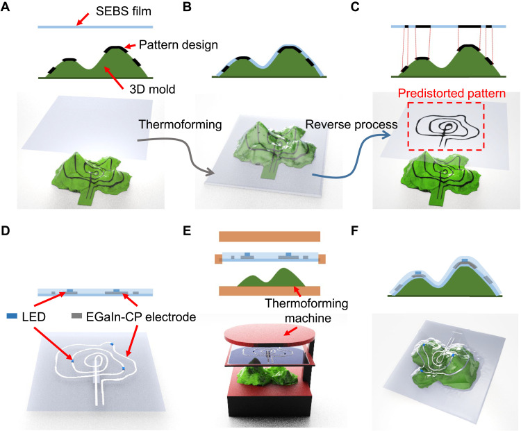
Fig. 2. Fabrication process of the PGT3DE.
(A) Design of 3DE circuit pattern on 3D mold. (B) Thermoforming simulation. (C) Predistorted pattern generation. (D) Patterning the EGaIn-CP electrode and mounting electronic devices on 2D planar SEBS film based on the predistorted pattern. (E) Thermoforming process. (F) Fabricated 3DE.

