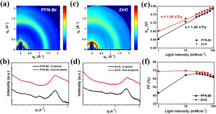
Figure 6.
(a–d) 2D GIWAXS patterns and line‐cut profiles of PTB7‐Th:PC71BM blend films coated on PFN−Br electron transporting layer (a,b) and ZnO electron transporting layer (c,d). (e,f) Light intensity‐dependent photovoltaic parameters of both devices: (e) VOC; (f) FF. Reproduced with permission from ref. [80]; copyright 2020, Elsevier.

