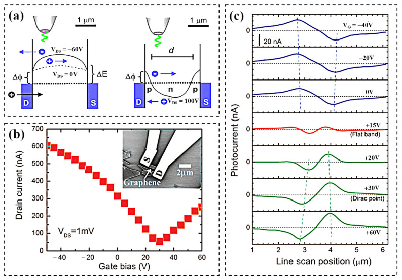
Figure 2.
Photovoltaic Effect. (a) Band diagrams at VGS = 0 V (dashed line) and VGS = −60 V (solid line) were obtained by numerical integration of the photocurrent profiles. describes the pinning of the Fermi level. Arrows indicate the flow of electrons and holes. (b) Electrical transport characteristic of a graphene transistor (drain current vs gate bias) at a drain bias of 1 mV. Inset: Scanning electron micrograph of the graphene transistor. (c) Photocurrent line scan profiles under different biases. (a) Reproduced with permission from [44]. Copyright American Physical Society, 2009. (b) and (c) reproduced with permission from [45]. Copyright 2009 American Chemical Society, 2009.

