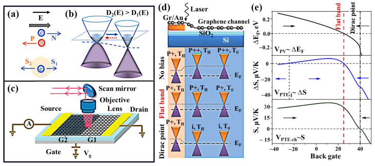
Figure 4.
Photothermoelectric Effect. (a) In the top panel, the built-in electric field picture for photocurrent generation at a p–n junction. The direction of the field E is defined along the direction of electron movement. In the bottom panel, hot carrier diffusions at a material interface with different S1 and S2. (b) Aligned Fermi level of the bilayer (left) and single layer (right) graphene. D(E) is the density of states. The blue and red dashed arrows represent the electron flow direction induced by the built-in electric field and by the thermoelectric effect, respectively. (c) Schematics of the experimental setup and device geometry. (d) Schematic of a graphene/Au interface and associated band diagrams for various gating conditions. (e) Calculated gate voltage dependence of Fermi level difference (top) and Seebeck coefficient difference (middle) between the Gr/Au and Gr/SiO2 areas and gate voltage dependence of Seebeck coefficient for the graphene channel (bottom). (a–c) reproduced with permission from [48]. Copyright American Chemical Society, 2009. (d,e) reproduced with permission from [40]. Copyright Nature Publishing Group, 2018.

