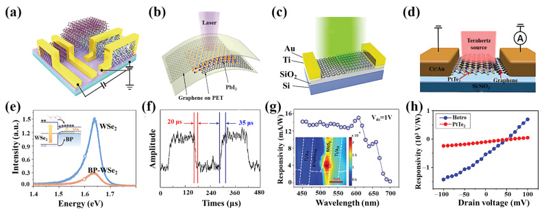
Figure 9.
Heterostructure photodetector. (a) BP–WSe2 heterostructures schematic. Schematic band diagram of BP–WSe2 heterostructures. (b) schematic of photoelectric measurement of the flexible device with near-ultraviolet laser source. (c) Schematic of lateral graphene–MoS2 heterostructure Schottky photodetector under the illumination. (d) Schematic representation of the electrical configuration for the bow-tie-type PtTe2-based THz detector. (e) PL spectra of monolayer WSe2 and the BP–WSe2 heterostructure under an incident laser. Inset: Schematic band diagram of BP–WSe2 heterostructures. The dashed line denotes the Fermi energy of BP and WSe2. (f) Fast device photoresponse, giving the rise and decay time, respectively. (g) Spectral responsivity for the detector. The absorption for the light of the device is mainly limited to the bandwidth of MoS2, corresponding to the test in the inset. Inset: scanning photocurrent mapping of the detector. (h) The voltage responsivity of the two devices under different biases at 0.12 THz. (a,e) reproduced with permission from [10]. Copyright Nature Publishing Group, 2019. (b–d,f–h) reproduced with permission from [94,98,102]. Copyright Wiley, 2018,2019.

