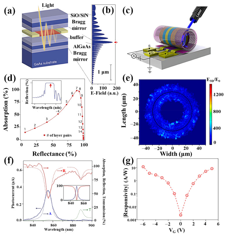
Figure 11.
Optical microcavities. (a) Schematic drawing of a graphene microcavity photodetector. Distributed Bragg mirrors form a high-finesse optical cavity. The incident light is trapped in the cavity and passes multiple times through the graphene. (b) Electric field amplitude inside the cavity. (c) Schematic diagrams of the 3D GFETs after the roll-up. (d) Calculated dependence of optical absorption in a single layer graphene sheet on the reflectivity of the top mirror. (e) The simulated distribution of the electric field magnitude near a 3D GFET with one rolled-up winding. (f) Spectral response of the single-layer graphene device. The dashed lines show calculation results: reflection R (red), transmission T (green), and absorption A (blue). The solid lines are measurement results: reflection (red), photocurrent (blue). Inset: Theoretical result for normal incidence light. (g) The gate-voltage-dependent responsivity of the 3D GFETs under VDS = 0 V. Reprinted with permission from [107,148]. Copyright American Chemical Society, 2012,2018.

