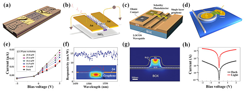
Figure 12.
Optical waveguides. (a) Schematic of the graphene/silicon-heterostructure waveguide photodetectors. (b) Schematic of the device. The silicon bus waveguide fabricated on a silicon-on-insulator wafer is planarized using SiO2. (c) Schematic of Si-SLG Schottky photodetectors integrated with photonic waveguides. (d) A schematic of an MRR-integrated MoTe2 photodetector. (e) Dark and illuminated current versus bias voltage of the same device as under different incident light powers. (f) Broadband uniform responsivity over a wavelength range from 1450 nm to 1590 nm at zero bias. Inset: simulated electric field of the TE waveguide mode. (g) Finite element simulated optical intensity profile of an SPP waveguide mode supported by an M-SLG-Si structure. (h) Typical I–V characteristics (semi-logarithmic plot) of the Au/MoTe2/Au diode showing around two orders of magnitude enhancement for light (red) over dark (black) conditions. (a,b,d–f,h) Reproduced with permission from [111,152,153]. Copyright Nature Publishing Group, 2013, 2019. (c,g) Reproduced with permission from [154]. Copyright American Chemical Society, 2016.

