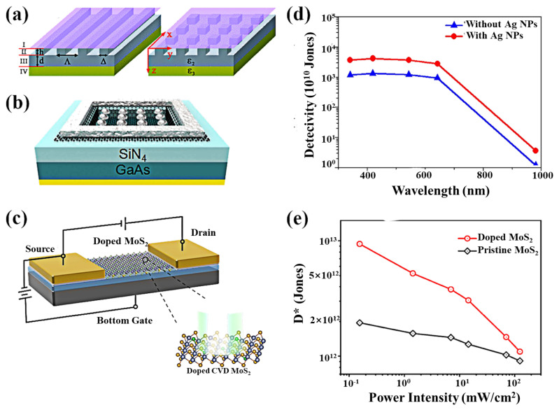
Figure 13.
The 2D materials-based plasma photodetectors. (a) Schematic view of a graphene monolayer supported on a 1D and 2D SWDG with thickness h, period, and strip/cylinder size. (b) Schematic diagram of graphene/GaAs photodetector with AgNPs. (c) Schematic diagram of the structure for the doping CVD MoS2 photodetector. (d) Detectivity of the graphene/GaAs photodetector with and without 100 nm AgNPs under zero bias voltage at five excitation wavelengths. (e) Power intensity dependence of D* for the two photodetectors. (a) Reproduced with permission from [161]. Copyright American Physical Society, 2012. (b,d) Reproduced with permission from [113]. Copyright Elsevier, 2018. (c,e) Reproduced with permission from [106]. Copyright American Chemical Society, 2019.

