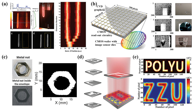
Figure 14.
(a) Image realized from an advanced dual-band vertical heterostructure GaSe/GaSb linear array photodetector. (b) Left: image sensor array based on graphene-complementary metal-oxide–semiconductors (CMOS) integration; right: near-infrared (NIR) and short-wave infrared (SWIR) image of a rectangular block covered in fog, behind a silicon wafer, and a glass of water. (c) 2D scanning imaging of the concealed metallic nut in an envelope. (d) Left: schematic illustration of the experimental setup for the integrated device to record infrared light imaging sensing. (e) The resulting images of “POLYU” and “ZZU” under 4.55 and 10.6 µm illumination, respectively. (a) Reproduced with permission from [165]. Copyright Wiley, 2017. (b) Reproduced with permission from [166]. Copyright Nature Publishing Group, 2017. (c) Reproduced with permission from [102]. Copyright Wiley, 2019. (d,e) Reproduced with permission from [41]. Copyright Wiley, 2020.

