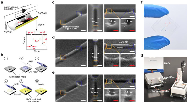
Figure 1.
Dual-nanopore time-of-flight (TOF) sensor. (a) Schematics of the dual-nanopore TOF sensor, which consists of a pair of in-plane nanopores poised on either side of a nanochannel used as the nanochannel column for nanoscale electrophoresis. Upon translocation of a dNMP molecule through the first in-plane nanopore, the nanochannel column, and the second in-plane nanopore sequentially, two consecutive current transient signals are generated. The time interval between the two current pulses corresponds to the TOF of the dNMP molecule through the nanochannel column. (b) Schematics of the device fabrication process: fabrication of Si master mold (1); fabrication of a UV resin mold via replication from the Si mater (2-3); UV-NIL into a PEGDA substrate from the UV resin mold (4-5); and simultaneous thermal bonding with a PEGDA cover plate resulting in pore reduction (6). Top and tilted view SEM images of (c) Si master mold, (d) the UV resin mold, and (e) the UV-imprinted PEGDA substrate. Scale bars, 100 nm in white and 50 nm in red. (f) A photograph of the TOF nanopore sensor fabricated by NIL. (g) TOF measurement system used included a sample holder, a custom current amplifier, and a data acquisition (DAQ) system. The current amplifier consists of a standard topology transimpedance amplifier (TIA) that is battery powered with a gain of 100 nA·V−1 and a single-pole −3dB bandwidth of 10 kHz. The output of the TIA is digitized by a National Instruments, Inc. model NI PXIe-6341 DAQ system at a sampling rate of 250 ksps.

