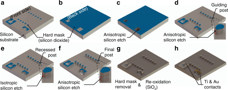
Fig. 7. Schematic illustration of the fabrication of the emitter substrate.
a Lithography on the front side and dry etching of silicon dioxide to define the hard mask. b Hard mask formation using lithography and dry etching of silicon dioxide on the backside of the substrate. c Anisotropic silicon etch on the backside of the substrate. d First anisotropic dry etching sequence of silicon on the front side of the substrate to form guiding posts. e Second isotropic etching sequence on the front side of the substrate to form the recess. f Third anisotropic dry etching sequence to finalize the guiding posts. g Removal of the hard mask and thermal re-oxidation forming an electrical insulation layer. h Evaporation of titanium and gold and lithographic structuring using a spray-coated resist, forming the metal contact pads

