
Fig. 1.
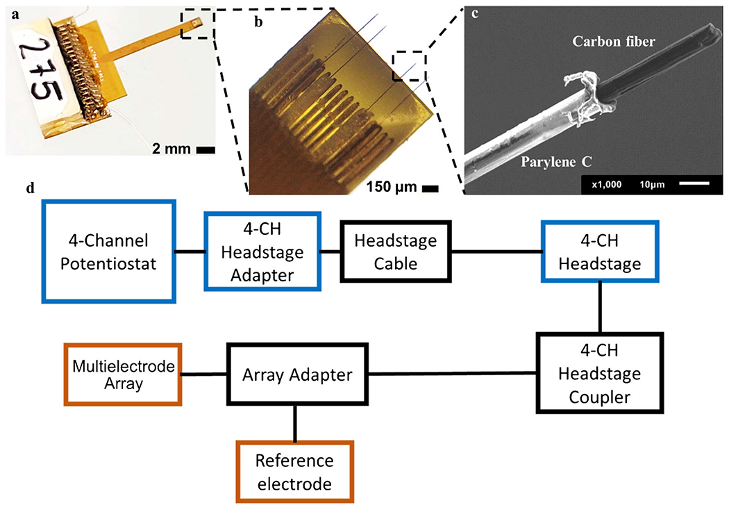
(a) The multielectrode array taken by a Samsung camera (Samsung Note 20 Ultra, 108-MP wide-angle camera). Approximate scale bar is shown. (b) The four carbon fibers of the multielectrode array viewed under a light microscope, at 20× magnification. (c) SEM image of a single fiber of the multielectrode array with a 10-μm scale bar. The carbon fiber (black) protrudes out, and the white insulating material is the Parylene C coating. (d) Connection schematic of multielectrode array showing the separate pieces of hardware that is required for adapting it to a commercial potentiostat. See ESM Fig. S1 for setup and parts photos