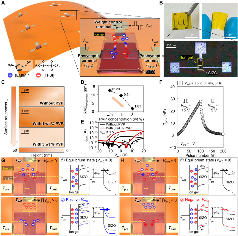
Fig. 1. Flexible synaptic device based on the SIZO/ion gel hybrid structure.
(A) Schematic images of the flexible synaptic device based on a SIZO/ion gel hybrid structure. (B) Flexible synaptic device array with a size of 3 × 3, which was fabricated directly on the PVP-coated PI substrate and the OM image of the magnified single device. (C) AFM mapping images of the SIZO surface without/with the insertion of the PVP buffer layer. (D) Calculated RMSroughness values with respect to the PVP concentration. (E) Static Ipost-VWC characteristic of the synaptic device without PVP buffer layer (black) and 3 wt % PVP buffer layer (wine). (F) Conductance response of the flexible synaptic device according to the continuous VWC pulses, where the pulse width and frequency were fixed as 50 ms and 5 Hz, respectively. (G and H) Weight update mechanism of the SIZO/ion gel synaptic device when the positive (G) and negative VWC (H) was applied, respectively. The left panels are illustrations of the ion movement in the SIZO/ion gel synaptic device, and the right panels are the energy band diagrams according to the applied VWC (photo credit: Jeong-Ick Cho, Sungkyunkwan University).

