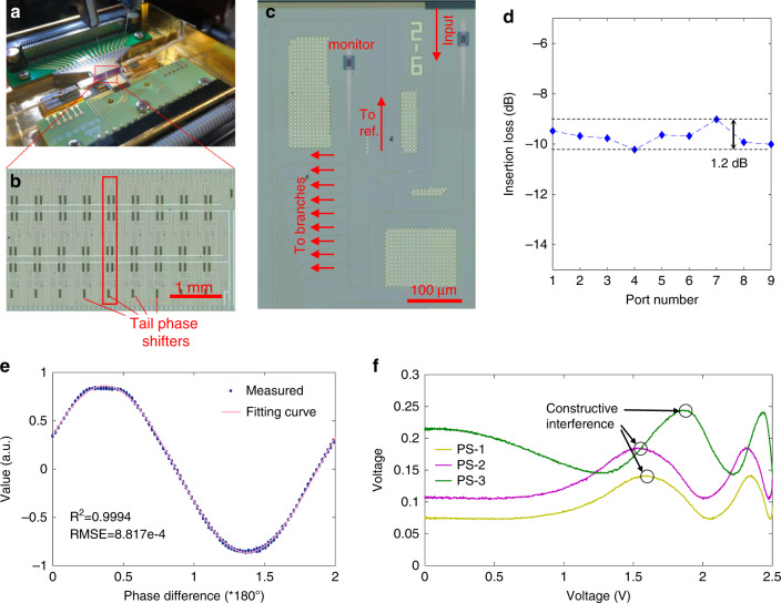
Fig. 2. Chip characterization results.
a The packaged OCDC with periphery circuits. b The top view of the OCDC. Modulating branches are located vertically as the red block shows. Every modulator contains four phase shifters, two of which are used to conduct push–pull modulation and the remaining two are used to control the bias voltage. Tail phase shifters are appended to compensate for the phase difference among branches. c The structure of light input and splitter. d Characterization of evenness of optical power splitting. e Modulator characterization with push–pull driven. The experimental result is fitted with a curve formulated by a * sin(b * x + c) + d. The information on fitting is also given in the plot. f The effect of constructive interference of three branches. Three curves are obtained one by one. Firstly, only the first branch is modulated to the highest transparency when the other two branches are closed. By changing the voltage on its tail phase shifter (PS-1), the yellow curve is shown. It denotes the interference result of branch 1 and reference branch. Secondly, keep the voltage on the PS-1 at the constructive interference point (black circled); modulate the second branch to its highest transparency; change the second tail phase shifter (PS-2). The purple curve is recorded. By operating the same process for the third branch, we obtain the green curve

