Figure 2.
Fabrication and characterization of the transparent nanowire sensor
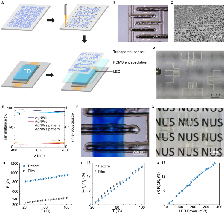
(A) Schematic of the fabrication process. AgNW film is selectively removed by laser-induced ablation to yield the desired pattern.
(B) Optical microscopy image of the sensor. White arrows show the nanowire path.
(C) SEM image of an intact region of the AgNW film after patterning.
(D) Image of the fabricated sensor array.
(E) Transmittance and absorbance spectra of the AgNW film before and after ablation following sensor design pattern.
(F) Optical microscopy image of the sensor. The bottom side of the sensor is marked in blue to highlight the transparency.
(G) Image of the sensor array on a lettered background.
(H) Resistance of the patterned sensor and AgNW film as a function of temperature.
(I) Relative change in resistance as a function of temperature.
(J) Relative change in resistance of the integrated sensor as a function of electrical power input to the LED array in free space.

