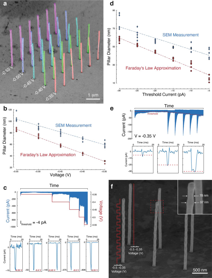
Figure 2.
Voltage and set point control of the printing process. (a) False color SEM image of a 5 by 6 array of pillars with a height of 3 μm. The overlaid text indicates the voltage at which the pillars of the respective line were printed. (b) Printed pillar diameters as a function of printing voltage as measured (from SEM image in (a), blue diamonds) and calculated (red circles) from Faraday’s law of electrolysis. The dotted lines show the linear trend relating pillar diameter and printing voltage. (c) Current traces for the voltage test (top) and individual peaks at different voltages. (d) Printed pillar diameters as the function of threshold current. (e) Current trace of pillars printed at different threshold set points (top) with close ups of individual current peaks at thresholds of −5, −20, and −30 pA, as indicated by the red dotted lines. (f) SEM image of pillars with (front row) and without (rear row) diameter modulation printed with a pipette with an opening size of about 50 nm. All pillars were printed layer by layer with voxel heights of 100 nm. For the front row the voltages were alternated between −0.5 and −0.35 V, as illustrated with the red solid lines along two pillars. The rear row was consistently printed with −0.5 V. By changing the voltage the voxel diameter is changed by 19 nm ranging from 78 nm (±1.7 nm, −0.35 V) to 97 nm (±1.7 nm, −0.5 V).

