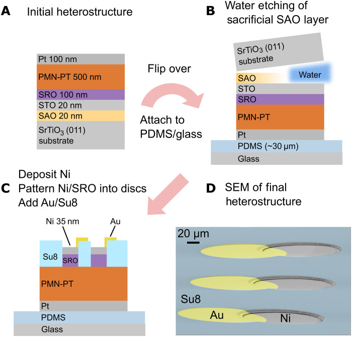
Fig. 2. Fabrication of single-crystal (011)-oriented PMN-PT membrane heterostructures.
(A) Initial thin-film heterostructure consisting of PLD-grown SAO/STO layers and sputter-deposited SRO/PMN-PT/Pt layers. (B) After attaching the heterostructure Pt-side into PDMS/Glass, the SAO sacrificial layer is etched by H2O. (C) After removal of the STO buffer layer, Ni is deposited by sputtering followed by patterning of the Ni/SRO layers into 160-μm circles. The membrane heterostructure is completed by addition of the SU-8 protective layer and Au-lifted electrode layer. (D) SEM image showing the completed membrane device.

