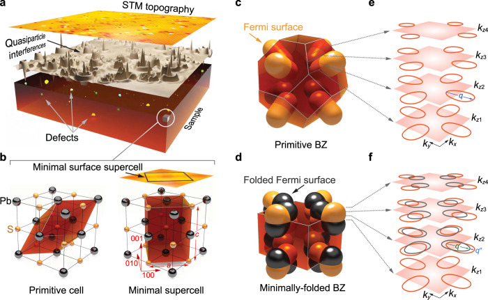
Fig. 1. Crystal structure and Brillouin zone of PbS.
a Visualization of quasiparticle interference in an isotropic material. A typical STM topography (obtained from PbS), exhibiting an atomically flat surface with a wide range of defects, is shown (Vset = 0.8 V, Iset = 0.2 nA). The (schematic) differential conductance map, which is proportional to the density of states, shows clear signatures of quasiparticle interference (QPI), evidenced as oscillatory patterns around defects in the surface, as well as sub-surface layers. These patterns contain information from the full electronic structure. b Difference between the primitive cell of the bulk and surface. Left: the primitive cell of the bulk FCC crystal structure shown in a unit cell of PbS. Right: minimal supercell with lattice parameters a and required to describe the surface. All crystallographic directions in the following refer to this supercell. c Schematic bulk Brillouin zone (BZ) of a cubic material with Fermi pockets centred at the zone boundaries, corresponding to the primitive cell shown on the left in b with a schematic electronic structure of an FCC material. The constant energy surface close to the top of the valence band in PbS is represented by pockets centred at the L-point (centre of the hexagonal faces). There are no states in the kz = 0 plane. d Brillouin zone corresponding to the minimal supercell shown on the right in (b), resulting in folding of the Brillouin zone and hence of the Fermi surface. e Cuts at different kz planes for the Fermi surface in (c). With decreasing kz the size of the contours increases. There is one dominant intra-pocket scattering vector q. f Decreasing kz planes for the Brillouin zone shown in (d). Due to the folding, there are two new intra-pocket scattering vectors, and q″, that do not exist in the bulk Brillouin zone.

