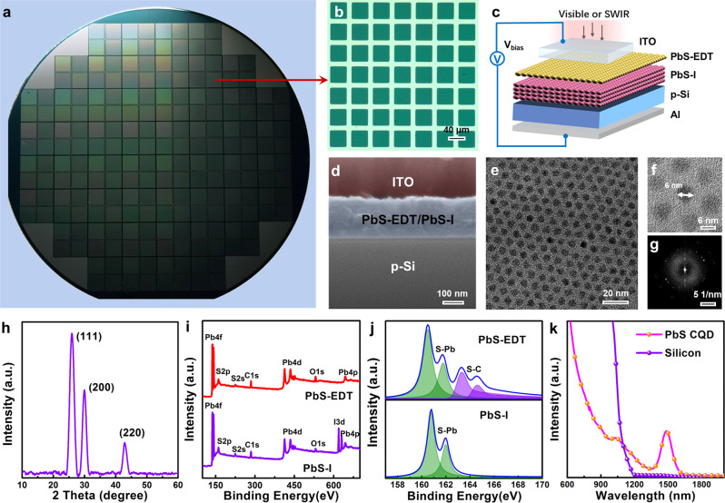
Fig. 1. Structure and material characterization of the PVTRI.
a PVTRI arrays in a 4-inch silicon wafer. b The optical microscope image to show a minimum pixel (40 × 40 μm) of the arrays. c The schematic device structure of a single Si:CQD PVTRI. At Vbias < 0, the p-Si substrate acts as the emitter while the base and collector are consisted of the ultrathin PbS n-CQD and p-CQD films, respectively. d The cross-sectional SEM image of the PVTRI. TEM (e) and HRTEM (f) images with the SAED patterns (g) of the PbS CQDs. h XRD analysis of PbS CQDs. XPS elementary composition (i) and S 2p peak spectra (j) of PbS-I and PbS-EDT. k Absorption spectra of the PbS CQDs and silicon.

