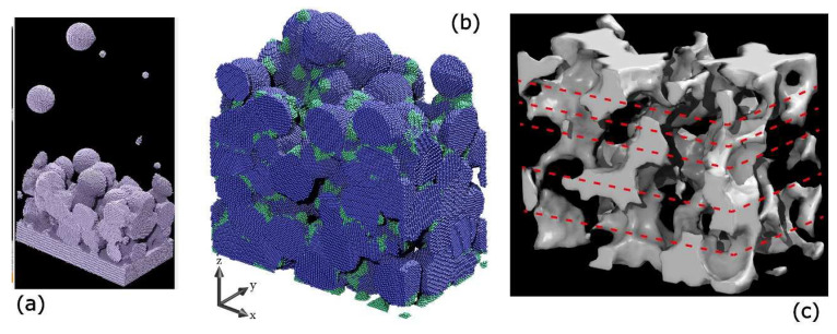
Figure 6.
(a) MD simulation snapshot of the landing process employed to build the virtual film. (b) Rendering of the final virtual NP thin film. The Ag atoms composing big (set B) and small (set S) NPs are colored in blue and green, respectively, following the same color definitions as in Figure 3b. The average film thickness is 28.6 nm. (c) Void structure. The white 3D scaffold represents the voids between the deposited NPs. The cell base size for all panels is 35 × 20 nm2. Panels (b,c) are adapted from ref. [25], further permission related to the material excerpted should be directed to the ACS.

