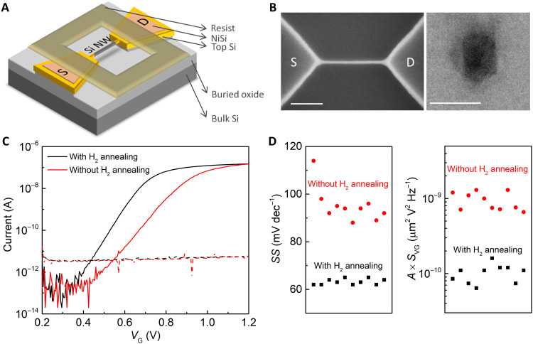
Fig. 1. SiNWFET fabrication process optimization.
(A) Three-dimensional schematic of a SiNWFET. The SiNW consists of a lightly p-doped region (gray) in the center and a heavily n-type region (yellow) on each side. (B) SEM image (left; scale bar, 100 nm) and cross-sectional TEM image (right; scale bar, 10 nm) of a SiNWFET with H2 annealing. (C) Typical transfer characteristics of SiNWFETs with and without H2 annealing measured in 1 mM KCl at VDS = 10 mV. The solid and dashed lines mean IDS and gate leakage current, respectively. (D) Summary of SS (left) and A × SVG at 10 Hz (right) of 10 SiNWFETs with and without H2 annealing measured in 1 mM KCl at VDS = 10 mV.

