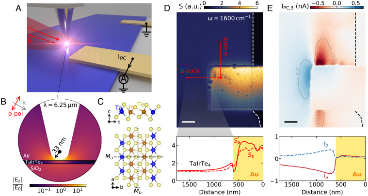
Fig. 1.
Near-field nano-optical and nano-photocurrent experiments on TaIrTe4. (A) Schematic for nano-infrared and nano-photocurrent measurements where the scattering (S) and zero-bias photocurrent () signals are collected simultaneously. (B) Simulation of the field enhancement for the z-component of the electric field (Ez) for a metallic tip ( 30-nm radius) close to TaIrTe4 surface with p-polarized incident light. (C) Crystal structure of TaIrTe4 for the side view (Upper) and top view (Lower). (D) Nano-infrared image of the scattering amplitude at (m) for a 12-nm-thick sample (Sample 1) at ambient conditions. (Lower) The linecuts along the a-axis (red solid line) and b-axis (red dashed line). (E) Nano-photocurrent map of the same region as in D, showing clear direction-switching pattern near the Au contact. (Lower) The linecuts of taken along the same paths as in D. (Scale bars in D and E, 600 nm.)

