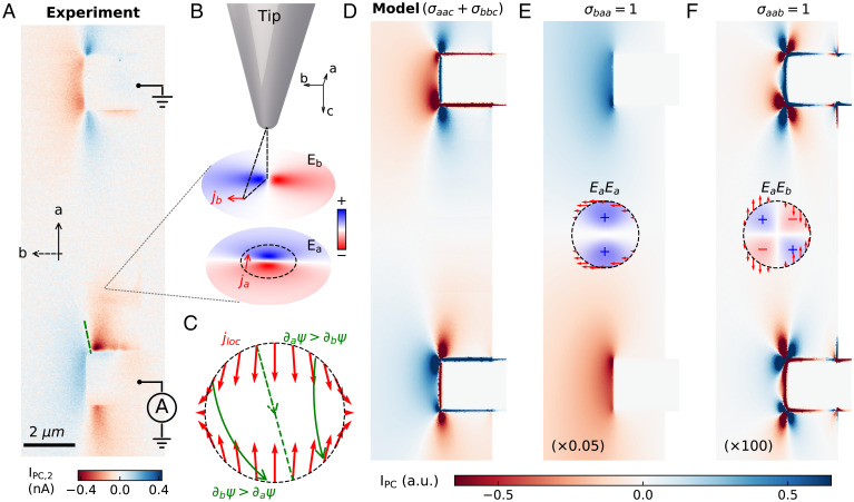
Fig. 2.
Nano-photocurrent experiment and modeling based on the SR theorem. (A) Nano-photocurrent map of Sample 1 at m, showing similar direction-switching behavior as in Fig. 1E. (B) Tip-mediated nonlinear photocurrent generation in the interior of the sample. Color plots are numerical calculation of the tip electric fields in the sample. (C) Magnitude and direction of the (red arrows) on a 100-nm-diameter circle centered at the tip position according to . Green arrows are schematics of the auxiliary field distribution . (D) Model simulation of the nano-photocurrent pattern with the profile in C, showing good agreement with the experiment. (E) Model simulation using , showing no direction-switching pattern near the contact. (Inset) The simulated distribution and the corresponding photocurrent (red arrows). (F) Model simulation using , showing more sign changes near the contacts compared to the experiment in A. (Inset) The simulated distribution and the corresponding photocurrent (red arrows). The magnitudes of the simulated photocurrent in E and F are scaled by 0.05 and 100 times, respectively. a.u., arbitrary units.

