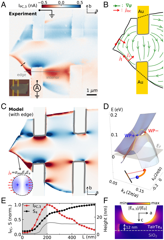
Fig. 3.
Boundary photocurrent in TaIrTe4. (A) Experimental photocurrent map in a four-terminal device (Sample 2), displaying direction-switching real-space pattern near the ground (top left) and collecting (bottom left) contacts. The two contacts on the right are floated. (Inset) An optical image of the device. (B) Simulation of the auxiliary field (green arrow) for Sample 2 under the SR scheme. Red arrows indicate local photocurrent generated near the boundary of the sample. (C) Model simulation of the nano-photocurrent pattern with the profile in Fig. 2C for the interior and additional boundary photocurrent contribution (Inset), showing good agreement with the experiment. (D) Band structure of TaIrTe4 showing two of the four Weyl points at around 0.1 eV above the Fermi energy (EF). (Bottom Inset) The finite projection of Fermi-arc states on a mirror-symmetry breaking edge (black line). (E) Photocurrent (red) and scattering amplitude (black) along the black dashed line in A. The photocurrent is peaked at the physical edge ( nm). The gray solid line is the corresponding topography profile. (F) Numerical simulation of the in-plane electric field (Ea) in the ac-plane (side view) for tip position located 40 nm away from the sample edge.

