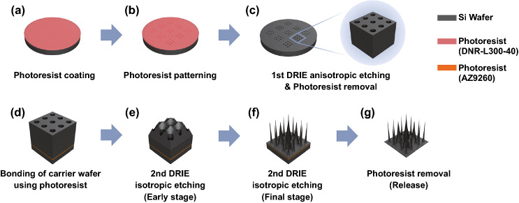
Fig. 1.
Schematics of fabrication steps of the microneedle arrays. a Photoresist (DNR-L300-40) coating on a processing Si wafer. b Patterning the photoresist as a masking layer for following deep reactive ion etching (DRIE). c Anisotropic etching (the 1st DRIE) of Si and subsequent removal of the photoresist. Inset shows magnified view of microwells formed by the anisotropic etching. d Bonding a carrier wafer under the processing wafer using another photoresist (AZ9260). e, f Isotropic etching (the 2nd DRIE) of Si microstructures. The microstructures at early (e) and final (f) stages are shown. g Release of the fabricated microneedle arrays from the carrier wafer by removing the bonding photoresist

