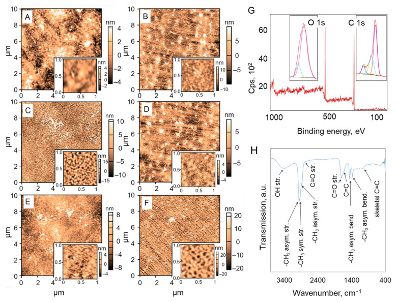
Figure 2.
Surface morphology and chemical composition of plasma polymer coatings with a thickness of 500 nm. (A–F) Representative atomic force microscope (AFM) micrographs of surfaces of coatings deposited on PET substrata (A) at 10 W (B), 15 W (C), 20 W (D), 25 W (E), and 30 W (F). Scanning area for the main image is 10 × 10 µm, scanning area for the insets is 1 × 1 µm. (G) X-Ray Photoelectron Spectroscopy (XPS) wide spectrum for coatings deposited at 15 W. The inset shows the high-resolution scans for oxygen and carbon. (H) Fourier Transform Infrared (FTIR) spectrum for coatings deposited at 15 W.

