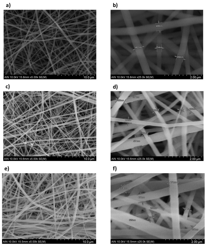
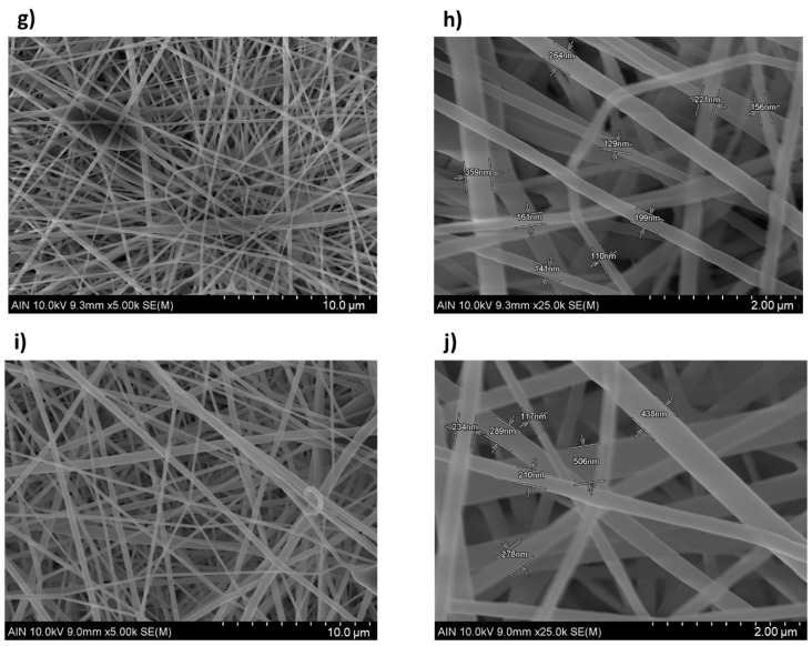
Figure 10.
Scanning electron microscopy (SEM) images representing the surface morphology of the electrospun mats for sample S1 (a,b) (500 µL/h and 13.2 KV), S2 (c,d) (1000 µL/h and 15.3 KV), S3 (e,f) (2000 µL/h and 17.7 KV), S4 (g,h) (3000 µL/h and 19.5 KV), and sample S5 (i,j) (5000 µL/h and 20.5 KV) at the scale of 10 µm (a,c,e,g,i) and 2 µm (b,d,f,h,j), respectively.


