Figure 2.
The single-bit counter design
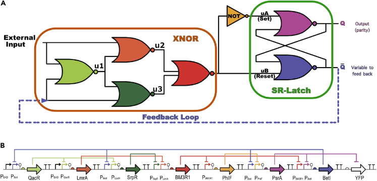
(A) Circuit design diagram for the single-bit counter. Shown is a seven NOR-gate implementation of the parity checker. This parity checker is a single-bit counter that contains two components. An XNOR component is shown inside the orange box, and an SR-latch component is shown in the green box. The design has a feedback loop from to the XNOR gate. The other input of the XNOR gate is the external input signal. The output of the single-bit counter is , which is the parity of the external input.
(B) A genetic network implementation of a single-bit counter which consists of insulated gates. The diagram shows the promoter-gene-repressor network of one possible plasmid implementation in an E. coli system. Repressor colors shown in this genetic construct are matched with the gate colors shown in (A). All the terminators are shown as a black “TT”.

