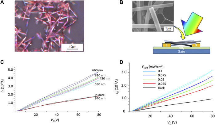
FIGURE 6.
(A) Optical microscopy image and (B) schematic diagram of OFET device of C60/3,5-TPP, inset: scanning electron microscopy (SEM) image of C60/3,5-TPP. (C) Wavelength dependence of the output characteristics of a C60/3,5-TPP phototransistor at VG = 80 V when illuminated with different LEDs (Elight = 0.1 mW/cm2). (D) Output characteristic curves of the phototransistor based on C60/3,5-TPP at VG = 80 V when illuminated with 660 nm light of different intensities (Elight) (Reproduced from Wakahara et al. (2020) with permission from American Chemical Society, Copyright 2020.).

