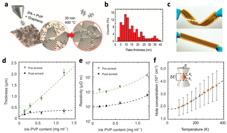
Figure 3.
Deposition and characterization of the graphene thin films: (a) deposition and annealing scheme of the exfoliated few-layer graphene flakes suspended in an IPA/PVP solution; (b) AFM thickness distribution of graphene flakes after annealing. (c) Photographs of an inkjet-printed device consisting of 20 silver and graphene legs bent (above) and as is (below); thermoelectric and transport characterization of graphene films: (d) thickness, (e) resistivity as a function of ink PVP concentration pre- and post-annealing; (f) post-annealing charge concentration with band overlap energy δE = 28.1 ± 2.3 meV as illustrated in the inset for two parabolic bands. Reprinted with permission from Ref. [44], Copyright 2018 John Wiley and Sons.

