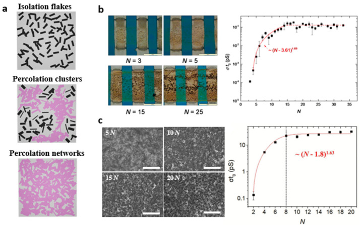
Figure 9.
(a) Schematic of percolation theory: isolation flakes, percolation clusters, percolation networks. (b) Optical micrograph of the printed MoS2 transistors on Si/SiO2 wafers with different printing passes N; conductivity variation of the printed BP films with respect to N. Reprinted with permission from Ref. [36]. Copyright 2014 John Wiley and Sons. (c) SEM images of BP films printed at 5 N, 10 N, 15 N, and 20 N (Scale bar = 10 µm); conductivity variation of the printed BP films with respect to N. Reprinted with permission from Ref. [22]. Copyright 2021 John Wiley and Sons.

