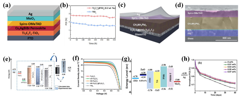
Figure 21.
(a) Schematic diagram of the device. (b) The measured PCE of the device. Reproduced with permission from Reference [185]. Copyright 2021, American Chemical Society. (c,d) Schematic diagram and SEM image of the device, respectively. (e) The energy band diagrams of each layer. (f) The J-V curve of the device with various ETLs. Reproduced with permission from Reference [186]. Copyright 2021, Royal Society of Chemistry. (g) The energy band diagrams of employed materials. (h) The stability values without the encapsulation under ambient conditions. Reproduced with permission from Reference [187]. Copyright 2021, Elsevier B.V.

