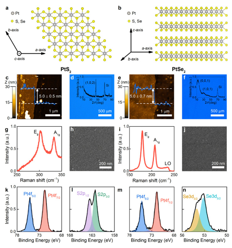
Figure 1.
Characterization of PtS2 and PtSe2 films. Crystal structure of PtS2 and PtSe2 from different views along (a) (001) and (b) (210) directions. AFM topography mappings and cross-sectional profiles of the edge of (c) PtS2 and (e) PtSe2. Optical images of (d) PtS2 and (f) PtSe2 on top of 300 nm SiO2/Si substrate. The insets show XRD diffraction patterns for PtS2 and PtSe2, respectively. Raman spectra at excitation wavelength λ = 632.8 nm of (g) PtS2 and (i) PtSe2 show characteristic Raman modes Eg and A1g. Note that PtSe2 also has an additional peak labelled LO (longitudinal optical) resulting from the overlap between infrared active modes Eu and A2u [27]. SEM images of (h) PtS2 and (j) PtSe2. XPS spectra of (k,l) PtS2 and (m,n) PtSe2.

