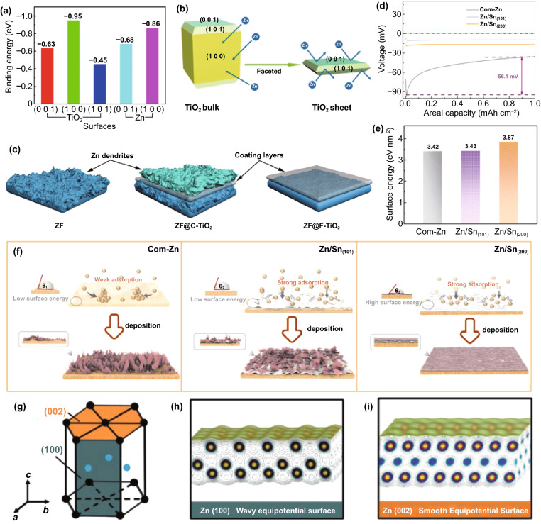
Fig. 9.
a Calculated binding energies of Zn atom with different facets; b Schematic illustration of the interaction between Zn and anatase TiO2 with different exposed facets; c Schematic illustration of the Zn plating process with different coating layers [86]. d Voltage profiles of Zn deposition on Com–Zn, Zn/Sn (101), and Zn/Sn (200) at a current density of 1 mA cm−2 and a capacity of 1 mAh cm−2; e The calculated surface energy on different electrodes; f Schematic illustration of Zn deposition process on Com–Zn, Zn/Sn (101) and Zn/Sn (200) [91].
Copyright 2020, Wiley–VCH. g The structure of metal Zn; Surface atomic arrangement and electron equipotential plane of h Zn (100) and i Zn (002) [92]. Copyright 2021, Wiley–VCH

