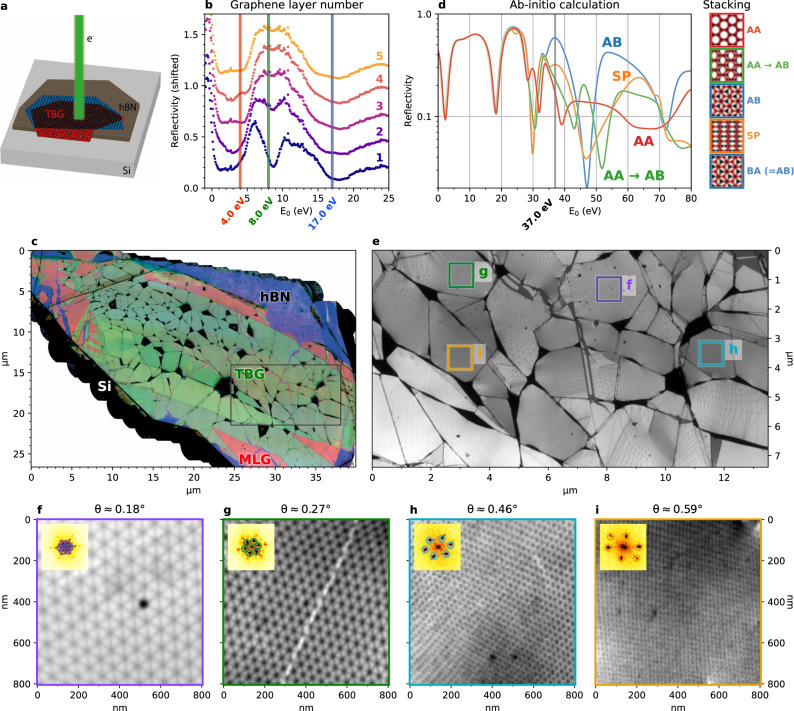
Fig. 1. Device-scale imaging of TBG.
a Schematic of the sample, with two twisted graphene flakes (TBG) on top of a hexagonal boron nitride (hBN) flake on a silicon (Si) substrate. b Local spectra that were used to determine the graphene layer count. Vertical lines indicate the imaging energies used for panel (c), the number of graphene layers for each spectrum is indicated on the right. c Stitched composite bright field overview of a sample using 4, 8, and 17 eV as imaging energies in red, green, and blue respectively (see main text for color interpretation). Visible defects include folds in black, tears, where the monolayer (red/pink, indicated as MLG) or even bare hBN (blue, purple) shines through, bubbles (bright), and some polymer residue in the lower and upper right (dark speckles). The black rectangle indicates the area shown in panel (e). d Ab initio calculations of LEEM spectra of different relative stackings of bilayer graphene, 37 eV indicated. e Stitched bright field overview of the same sample imaged at E0 = 37 eV, for optimal stacking contrast, revealing the moiré patterns. f–i Crops of different twist angle areas from (e). Insets show Fourier transforms and the detected moiré peaks, with the average twist angle θ extracted from those indicated. All data shown in the main text have been collected from the sample represented in panel (c).

