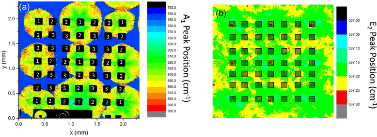
Figure 3.
(a) Raman map of the A1 (LO) peak on a 7 × 7 device reticle; the black areas are the regions are the metal contact to the anode. (b) Raman map of the E2 peak of a similar region. Translucent black boxes are drawn where the diodes are expected to be fabricated. The devices are divided into 3 positons labeled in (a): Postion 1, on a point of high crystal stress; Position 2, adjacent to point of high crystal stress thus still on a point of higher carrier concentration; Position 3, on a higher resistivity point away from the crystal stress points.

