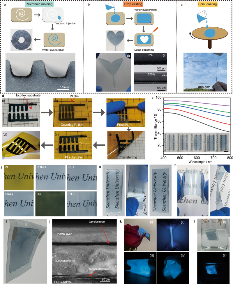
Fig. 4. Solution processing and patterning of SACP patterns and thin films for flexible or even transparent electrodes.
a Microfluid molding. b Drop casting. c Spin coating. d Transfer-printing of SACP patterns for lighting up an LED lamp from Ecoflex to PI substrate enabled by the difference of adhesion strength. e UV–vis spectrum and images of different transmittance SACP films. f Images of SACP films on various substrates by spin-coating. g Images of SACP films under repeating peeling tests by commercial test tapes. h Images of adhered PET film under bending and twisting. i Image of alternating current electroluminescence (ACEL) devices by applying SACP thin film as transparent electrodes. j Scanning electron microscope (SEM) image of the cross section of the ACEL devices. k Images of the ACEL device (i) under folding (ii), bending (iii) and wrinkling (iv). l Images of the ACEL device immersed in water for 24 h under bright (i) and dark (ii) backgrounds.

